The history of electronic design has been defined by repeated waves of major technological change and accompanying business realignment. Many companies have foundered and disappeared when they were unable to anticipate and adjust to these powerful forces of change. Consequently, I am not alone in believing that now is the time to get ready for the next significant change to your electronic design flow, and even the way your company organizes and partitions design teams. I am convinced that designing a 2.5D or 3D multi-die stack will soon be coming to a project near you, and it will bring you face to face with physics domains and challenges that are new to many IC design teams. This conviction is based on real market data from key EDA solutions providers like Ansys who report that their multiphysics analysis tools were used on more 2.5/3D-IC design starts in 2020 alone than in the past 10 years combined.
Every time design technology changed it was done as a reaction to break through a wall, or bottleneck, that limited our progress towards ever bigger and more integrated systems. Looking back at how the semiconductor industry has accommodated these earlier paradigm shifts can teach us to better understand and adjust to this new inflection point around 3D design.

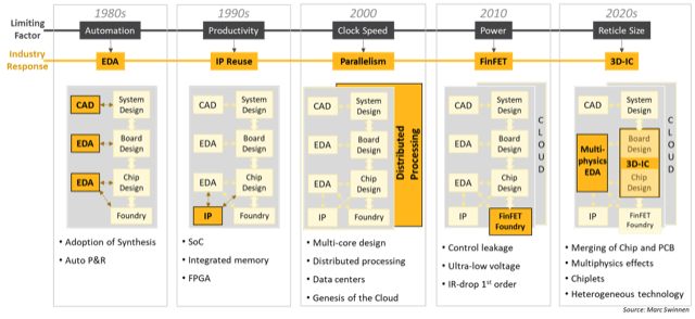
Fig. 1: History of technology bottlenecks in semiconductor design capability and how the industry has responded and changed in order to break through each time.
By the late 1980s, hand drawing of schematics and manual RTL creation were the limiting factors on taking advantage of Moore’s Law. The industry responded by adopting automation on an unparalleled scale and depth. EDA came of age with leaps in automation including logic synthesis, static timing analysis, and the automated place-and-route gate array ASIC design flow.
In the 1990s, the new bottleneck was designer productivity, and the industry reacted by developing extensive methodologies for design reuse. The intellectual property (IP) sector was born, and IP reuse became supported by all EDA tools and is now a standard component of every SoC. The business side was also realigned to reflect this change, with industry giants like Synopsys and Arm providing critical IP infrastructure to all IC designs.
The 2000s saw a technical plateau for the clock speeds that could be achieved for digital designs at <5GHz, and this was blocking the upward trend in compute power. The industry reacted by embracing parallelism and multi-core execution. EDA tools adjusted, not least by upgrading their algorithms to make use of the very parallelism that they were being used to design in microprocessors.
The most recent shift in the 2010s came from the rise of power management to a first-order concern, not just for battery-powered applications but for everyone, including even HPC datacenters. This is what drove the technology shift to finFETs, fully depleted SOI, and ultra-low operating voltages. Electronic design practice has similarly shifted to increased emphasis on low-power design and power integrity signoff as a key technology.
Which brings us to the present day where new silicon applications like GPUs, TPUs, and AI/ML chips are overflowing maximum reticle sizes and require huge amounts of closely integrated memory. The only way these high-end systems can achieve their power and performance goals is through the intimate integration of multiple dice on an interposer substrate (2.5D-IC) or by stacking dice directly on top of each other (3D-IC and HBM). And it’s not only the high end that is adopting 3D design. There are also strong economic reasons driving the disintegration of SoCs into a heterogeneous collection of smaller die that need to be integrated on a die-to-die substrate. This move to embrace “chiplet” design is still nascent, and not yet as mature as the more traditional 2.5D and 3D design, but is currently undergoing a lot of development efforts. The technology challenges faced by 3D-IC designers are significantly altering many of our assumptions about how to go about designing chips.
Here is a list of what I believe to be the top 10 major issues to consider when considering 2.5/3D-IC design:
Each of these points deserves a whole discussion in its own right, but 3D-IC is here today, and it will affect almost every step in the EDA and system design flow. I believe the companies that invest early and most rapidly adjust to this new electronic design paradigm will be the ones to reap the greatest benefits and outpace their competitors in the years ahead.
The highly anticipated GTC developer conference of AI chip giant Nvidia is about to be held, and the global trend of AI computing power is receiving attention. As UK chip architecture company Arm conti...
On the 18th, American chip company Nvidia unveiled its latest high-performance graphics processor (GPU) B200 based on the Blackwell architecture, which can be applied in the field of artificial intelli...
At the ISSCC 2024 held on February 18-22, TSMC brought another new technology. The full name of ISSCC is International Solid State Circuits Conference, which is recognized by the academic and industria...
On March 14th, Fast Technology announced that today, American chip startup Cerebras Systems has launched the worlds strongest third-generation wafer level AI acceleration chip, WSE-3 (Wafer Scale Engin...
On March 16th, Shi Ying, General Manager of China Products and Applications at Texas Instruments Semiconductor Company (hereinafter referred to as Texas Instruments), gave a speech at the China Electri...
According to a report from Fun Science website on the 14th, American chip startup Cerebras Systems has launched a new 5-nanometer wafer level Engine 3 (WSE-3) chip. The companys official website states...